
 Home
Home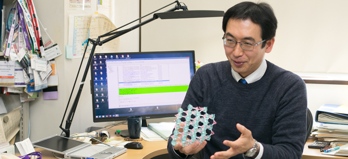
The interview series of "What We've Found Particularly Good About HU" proudly shares with you what's wonderful about Hiroshima University.
We’re setting the pace in the field of semiconductor nanotechnology
I belong to Hiroshima University’s Research Institute for Nanodevice and Bio Systems, which conducts research in the field of semiconductor nanotechnology. We routinely have numerous projects on the go: currently, we have about 50 joint research projects underway, along with 60 supported by the Nanotechnology Platform of the Ministry of Education, Culture, Sports, Science and Technology (MEXT).
Helping to sustain these projects are our two super-cleanrooms (rooms with very clean air). The highly innovative field of semiconductor nanotechnology has very demanding requirements for a clean environment.
Universities and research institutes other than Hiroshima University also have super-cleanrooms, but ours are in particularly active use. They’ve won such a reputation for their user-friendliness among researchers at other institutions that eminent researchers come to Hiroshima University from across the globe to conduct their experiments in our facilities. More than 30 years have passed since the founding of the Research Center for Integrated Systems, the forerunner of the Research Institute for Nanodevice and Bio Systems. Over the years, we’ve amassed an outstanding stock of know-how through our research into semiconductor devices and the development of related facilities and equipment.
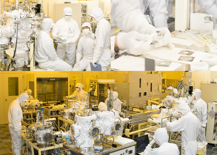
Associate Professor Kuroki and students conduct experiments in a super-cleanroom
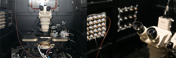
An electron-beam lithography system, that can achieve a circuit with the minimum line width of 6 nanometers (1 nanometer = 0.000001 millimeter)! The institute has more than 80 types of apparatus, including thin film deposition systems and measurement systems for nanodevices and its physical properties. It’s great to have access to all these devices in a single building.
With our lively bunch of students, we immerse ourselves in unfettered debate about our research
Most of our research is conducted jointly with industry and government, such as a project focused on developing semiconductor devices that directly control power to the motors of electric vehicles (power semiconductor devices). The Research Institute for Nanodevice and Bio Systems has more than 30 enrolled undergraduates and graduate students. It also attracts corporate researchers and engineers and I imagine that they find the ability to engage in various discussions here highly meaningful. I’m frequently overwhelmed by the boundless energy of our students. I get a steady stream of requests from students, asking if they can present their research at this international academic conference or discuss that experimental data. Being too conscious of one’s status as a faculty member or student leads to excessive formality in dealings with each other, which makes it difficult to engage in enthusiastic discussion of research. That’s a waste. I like an atmosphere in which we can debate with each other, concentrating on the core aspects of our research.
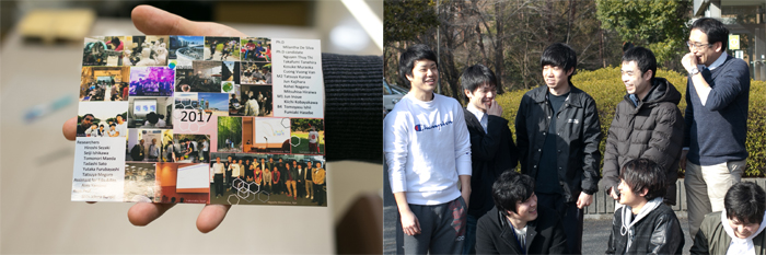
At his laboratory’s year-end party, Associate Professor Kuroki present everyone with a collage of photographs from academic society meetings and laboratory events over the course of that year.
Silicon carbide semiconductors could be used in decommissioning nuclear reactors, in space, or in medical care
I’m currently engaged in research and development focused on silicon carbide semiconductors, which is probably a term that you’re not used to hearing in everyday conversation. I’m researching semiconductor circuits that could make use of the features of these semiconductors in extreme environments, particularly in nuclear reactor decommissioning, space exploration, and precision medical instruments. Today’s semiconductors are vulnerable to radiation, so can’t be used for long periods in such environments. This research is essential to progress with the decommissioning of Fukushima Daiichi Nuclear Power Plant and planetary exploration, among others. We need to achieve results without delay. I hope to make full use of our research environment to gradually produce devices with bigger and bigger circuits, in order to contribute to society.
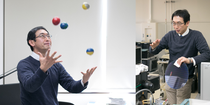
Associate Professor Kuroki juggles when he wants to gather his thoughts. Sometimes, 30 minutes or more can pass before he knows it, he says.
Profile
Completed the doctoral program at Hiroshima University Graduate School of Science. Took up his current post after holding a number of positions, including assistant professor at Tohoku University. Since 2013, he has undertaken joint research as a visiting researcher at KTH Royal Institute of Technology, Sweden.
Overview of Research
Associate Professor Kuroki’s research focuses on silicon carbide (SiC) harsh environment electronics and silicon thin-film transistors. He aims to open up new frontiers in space and deep underground, among others, by building silicon carbide integrated circuits that can operate even when exposed to radiation and in extreme heat environments. As well as receiving a grant from the Fund for the Promotion of Joint International Research (Fostering Joint International Research) for 2016-17 under the JSPS KAKENHI Grants-in-Aid for Scientific Research program, he is currently working with both Japanese and foreign researchers on research and development focused on silicon carbide devices that can be used in reactor decommissioning work at Fukushima Daiichi Nuclear Power Plant.
(Interview: February 2018)