The newly developed receiver chip with the world’s first mixed-signal baseband demodulator circuit
THine Electronics, Inc. (Tokyo Stock Exchange: 6769, “THine”), National Institute of Information and Communications Technology (“NICT”), and Hiroshima University, a national university corporation (“Hiroshima University”), jointly announced the successful development of 20 gigabits per second (20Gb/s) QPSK*1 wireless transmission technology with the world's first mixed-signal*2 baseband demodulator*3 technology, which would have a great advantage to achieve more power-efficient wireless data transmission for higher-speed appreciations.
THine was responsible for overall design and measurement, Hiroshima University for discussions on design and measurement, and NICT for discussions and measurement assistance.
Details of the technology was presented at the 2024 IEEE custom Integrated Circuits Conference (CICC) held from April 21st to April 24th in Denver, Colorado [1].
The results of this research pave the way of practical circuit implementations by newly-developed mixed-signal architectures for various applications that require higher-performance and more power-efficiency.
Newly developed technology
- Mixed-signal architecture realizes ultra-high-speed data transmission, improving power efficiency
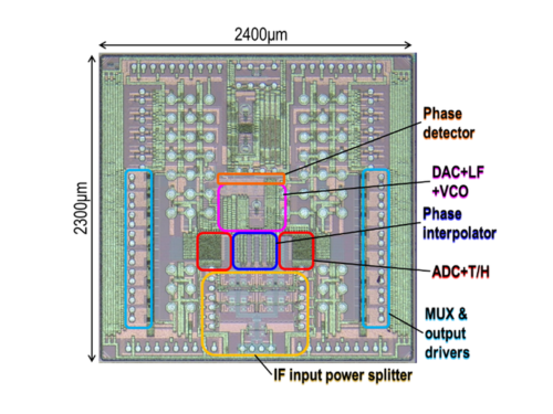
The research group has developed the world's first mixed-signal baseband demodulator circuit consisting of a high-speed, low-resolution ADC*4 and a small-scale DSP*5. This technology is expected to realize higher-data communications exceeding tens of Gb/s, achieving a superior power-efficient baseband demodulator circuit.
In general baseband demodulation circuits in high-speed wireless communications consist of a high-speed, high-resolution ADC and a large-scale DSP and, if used for such high-speed communications, the required performance of ADC and DSP results in extremely distorting power efficiency. The developed technology solves these problems.
- The receiver circuits with the baseband demodulator enables 20Gb/s QPSK data transmission
The developed receiver circuits the baseband demodulator and an FPGA*6 with logic circuits have achieved data transmission of 20Gb/s QPSK modulated signals. The functions implemented in FPGAs will be integrated into baseband receiver circuits in its practical application.
- Outline of the achieved circuits
The achieved technology simplifies the circuits by making the carrier*7 frequency an integer multiple of the symbol*8 carrier frequency, achieving ultra-high-speed data transmission by a unique circuit configuration with a mixed-signal QPSK Costas loop that integrates carrier, timing*9, and data recovery functions. The research group has achieved the high-speed, low-resolution ADC by implementing an 8-way interleaved 3-bit ADC (8x speed-up as the total circuits) with the sampling rate of 40-gigasample-per-second (40GS/s) and recovered data with the FPGA.
Note:
*1 QPSK: Quaternary Phase Shift Keying
*2 mixed signal: circuit that handles both analog and digital signals
*3 baseband demodulator: circuit that demodulates a modulated baseband signal (digital signal) transmitted wirelessly to the original baseband signal at the receiver side
*4 ADC: Analog-to-Digital Converter
*5 DSP: Digital Signal Processor
*6 FPGA: Field Programmable Gate Array
*7 carrier: radio wave used to transmit and receive signals
*8 symbol: unit of modulation signals used to put information on a radio wave
*9 timing: time information required to generate data
Background of the MIC R&D Project
The Ministry of Internal Affairs and Communications (“MIC”) of Japan aims to support the expansion of radio wave resources by conducting the program “Research and Development for the Expansion of Radio Wave Resources” to alleviate frequency congestion and for the effective use of radio waves, to enable ultra-large capacity wireless communications, and to promote the use of new frequency bands in order to meet the growing needs for new radio wave applications.
A part of this achievement is funded by MIC (JPJ000254).
Project name: “Research and development of terahertz wave transmission technology for ultra-large-capacity wireless LAN”
Sub-project theme (i) “Research and development of transceiver technology”
Reference
[1] Shunichi Kubo1, Yuji Gendai1, Satoshi Miura1, Shinsuke Hara2,3, Satoru Tanoi2, Akifumi Kasamatsu2, Takeshi Yoshida3, Satoshi Tanaka3, Shuhei Amakawa3, Minoru Fujishima3, “A 20Gb/s QPSK Receiver with Mixed-Signal Carrier, Timing, and Data Recovery Using 3-bit ADCs,” 2024 IEEE Custom Integrated Circuits Conference.
1THine Electronics, Inc., 2National Institute of Information and Communications Technology, 3Hiroshima University
Related links
-THine Electronics link
*Hiroshima Univesity is reposting this joint press release with the THine Electronics. Please see the link above for the original.
Related faculty members
Contact Information
THine Electronics, Inc.
Takeo Yamamoto
Tel: +81 (3) 5217-6660, E-mail: investors * thine.co.jp
(Note: Please replace * with @)
National Institute of Information and Communications Technology
-Research Contact:
Akifumi Kasamatsu
Director General, Koganei Frontier Research Center, Advanced ICT Research Institute
E-mail: kasa * nict.go.jp
-Media Contact:
Press Office, Public Relations Department
E-mail: publicity * nict.go.jp
(Note: Please replace * with @)
Hiroshima University
-Research Contact:
Minoru Fujishima
Professor, Graduate School of Advanced Science and Engineering,
E-mail: fuji * hiroshima-u.ac.jp
-Media Contact:
Public Relations Office
E-mail: koho * office.hiroshima-u.ac.jp
(Note: Please replace * with @)

 Home
Home